/article-new/2019/06/2020-iphone-triad.jpg?lossy)
Have you ever wondered what’s inside of your electronic devices? Today, we will uncover the mystery of the circuits that works inside — where they come from, how they are designed, tested and manufactured, from a very high level.
There are tons of electronic devices in the market, as advanced as your laptop, mobile phones, or gaming consoles. Or as simple as your lamp, or mobile phone charger.
If you open any of them up, you will see some printed circuit boards, PCBs. For those complicated ones, you will find multiple pieces of PCBs crammed in, working with each other.
3-Step Process
The design process for electrical engineers to test out ideas and make them into a printed circuit board for a product could be generalized into 3 steps.
- Start designing on something called breadboard
- Transition into a more permanent protoboard
- Finally, design and assemble PCBs
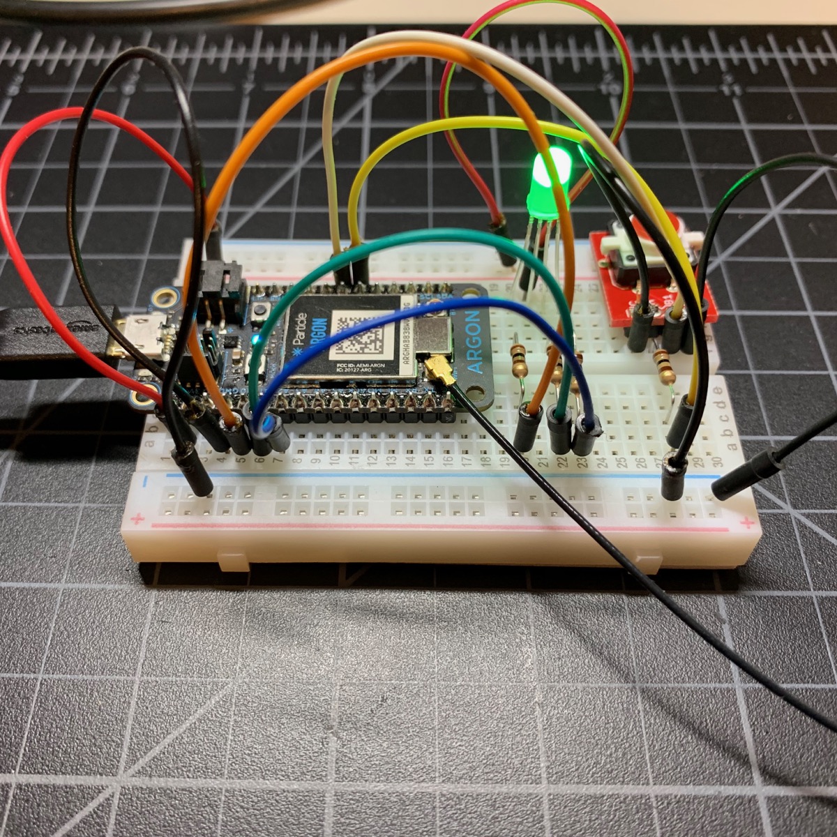
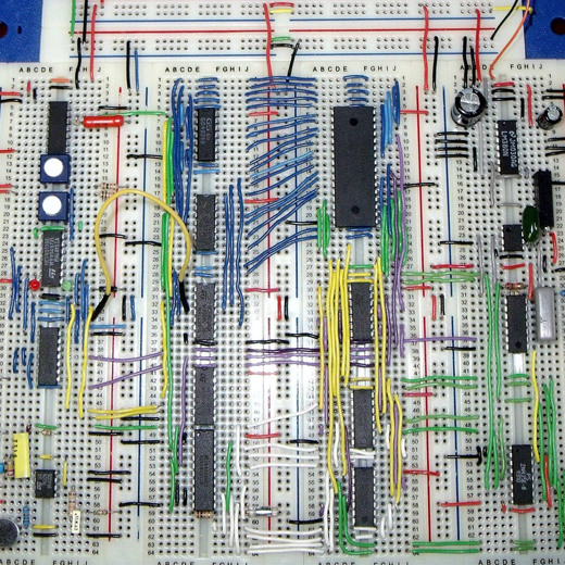
Breadboard — Implement initial design
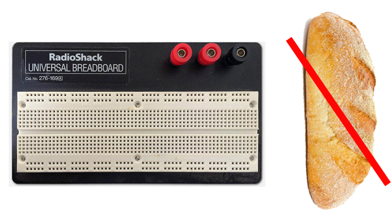
When electrical engineers got an idea for a product that require some circuits, they always start with something called “breadboard”. A breadboard in fact has nothing to do with a bread. It is a tool that people use to make electrical connections with pre-made “wires” underneath, so engineers can simply plug in things into the breadboard and make a circuit, instead of holding and touching components to each other.
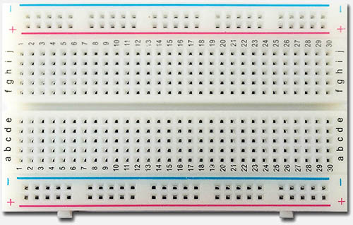
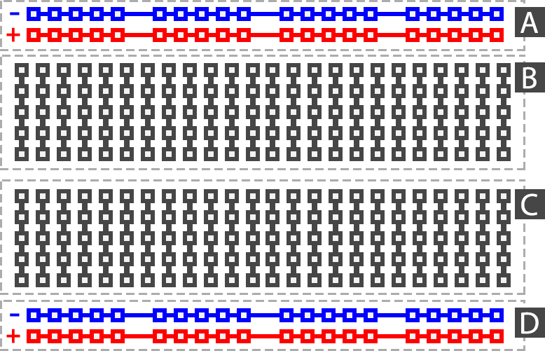
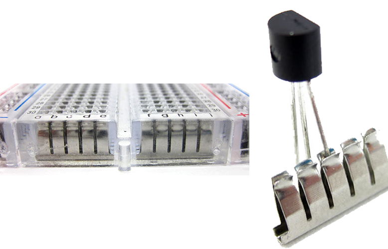
What’s underneath a breadboard is those metal clips that act like wires, between the component legs that are plugged in.
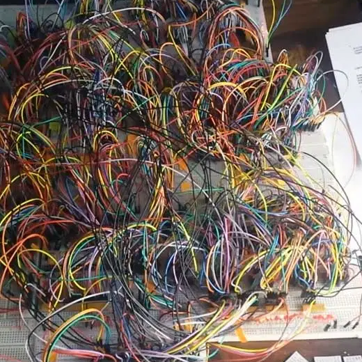
Now, there are many pros to using breadboards in the testing stage, but issues will arise if you are making a complicated system. although you can spend 5x longer to make everything clean, you will mostly run into endless troubles that are very difficult to debug.
Pros
- Cost effective
- Fast verification on idea feasibility
- Fast implementation into system
- Able to make last-minute changes
Cons
- A lot of wires
- Very large
- Hard to debug
- Unreliable connection
For example, you would never know if one of your wires is broken in its inside, or one of your thousands of wires accidentally got unplugged. Those issues will take you years to debug.
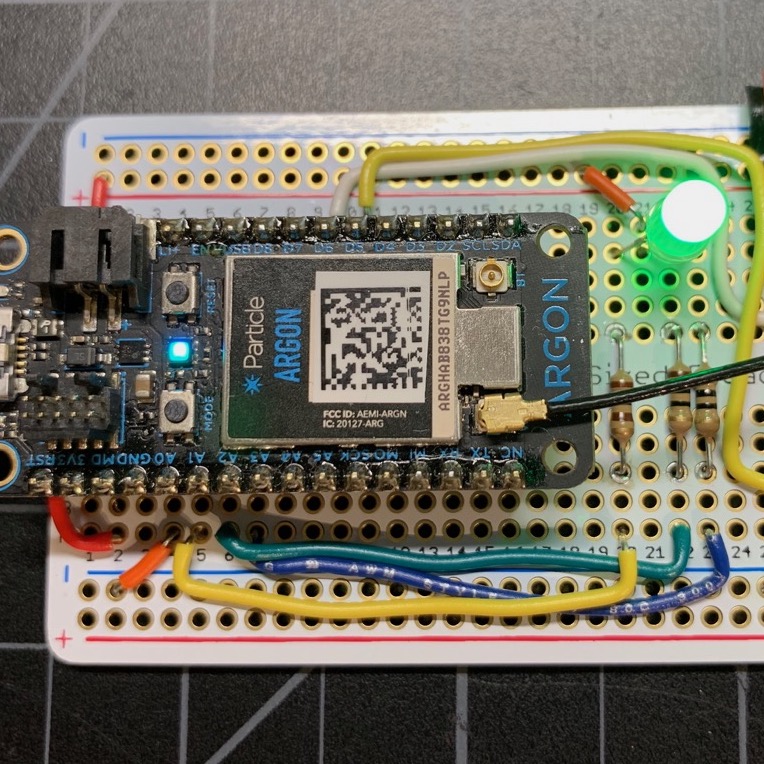
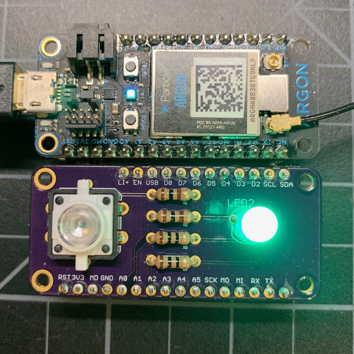
Protoboard — More permanent
So although it is a good initial step to breadboard but as you get closer and closer to realizing your product you don’t want those wires dangle around, but instead something more robust and reliable, and smaller in size that you can fit, or screw into somewhere more permanently.
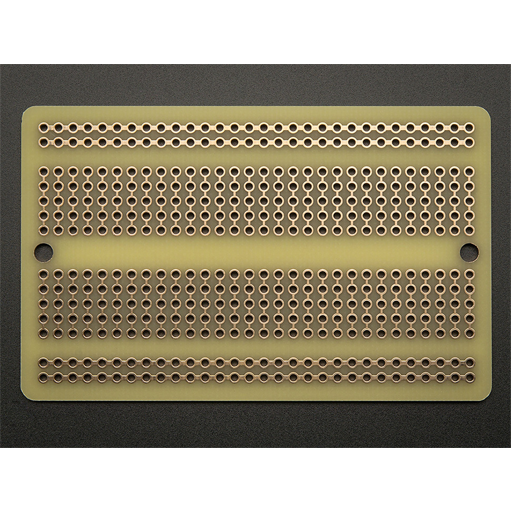
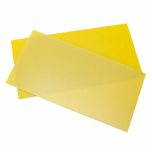
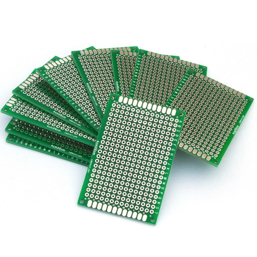
This is when protoboards come into play. They are a type of generic printed circuit board. Its base is a fiberglass plate.
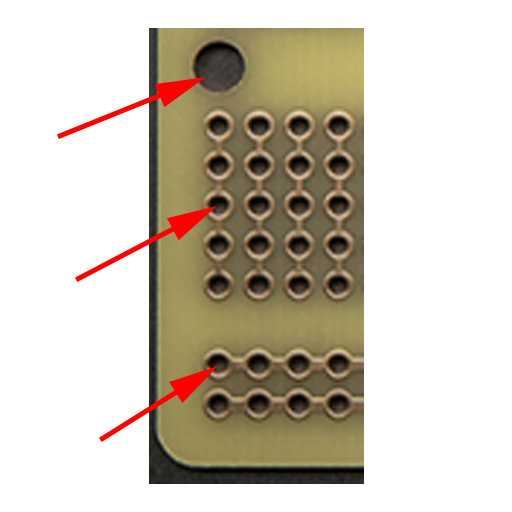
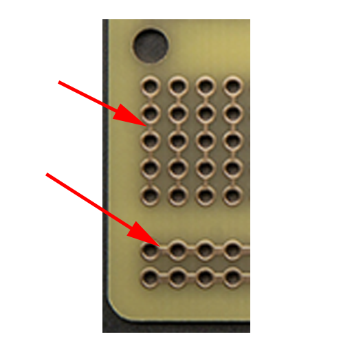
On the protoboard, you will see machine drilled holes for components to be plugged in, and conductive copper manufactured onto it acting as wires.
Now this may get you confused. How do you jump from plugging stuff into holes on breadboard into getting them permanently mounted on a PCB? This requires some operation called soldering . The idea is that you would melt something called “solder” that’s conductive, to create joints between your component’s leg, and the pad on the protoboard, or PCB.
Soldering
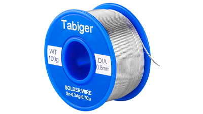
Use “solder” to create conductive joints
- Plug in the “soldering iron” and let it heat up
- Melt the “wire solder” upon touching the tip of the iron
- Liquid solder cools down and turns into permanent conductive connection
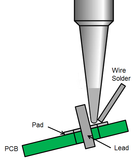
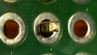
Instead of plugging into those clip-styled metals underneath the breadboard, now we are using this solder to “glue” the component’s leg onto the board, conductively. If you are interested, read more about soldering here.
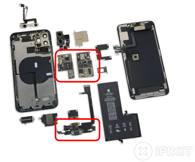
Printed Circuit Board (PCB) — The final product
Now you might say, well, protoboard is good. Its connection is permanent, and could be made small. But no! It’s not good enough for a product. Nobody is going to solder all the components in your phone on a protoboard and make it to work. We like machines doing the job not ourselves. Now PCB comes into play.
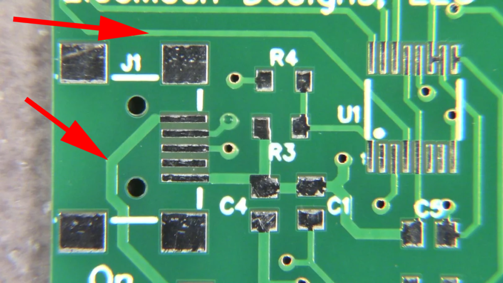
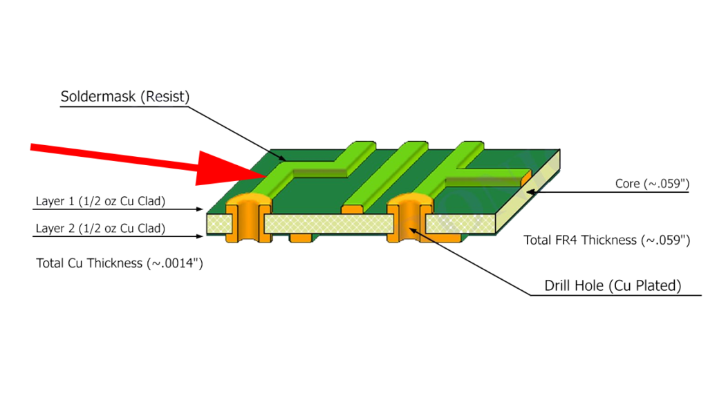
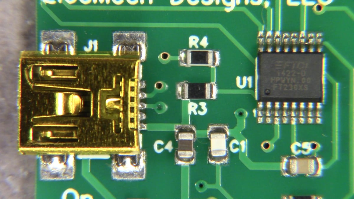
PCB is a piece of manufactured circuit board, with all the connections already printed precisely onto it, as you can see the lines laying down there and on the cross-section picture. They are conductive copper wires connecting points on the PCB.
With PCBs, it draws more clearly a line between manufacturing, and assembling. Engineers first design the board via some software tools, send to a factory to have it made, and receive what’s on the left below.
Now that’s not the end because it has no component on it. For the circuit to work, we need the chips and resistors on it. The PCB needs to be assembled. During assembly, the components are placed then soldered onto the PCB. For testings, engineers place and solder these components by hand, but usually during production, this process is highly automated with machines.

Conclusion — The design cycle
That’s it! I hope by now you have a picture on this prototyping to product process. Engineers start with a breadboard with their initial design. They can build it quick, mess around with it and correct stuff. Once engineers are ready, move onto a protoboard, and try to fit it into their system, and do more testing. If it’s a small project, they could also be just done with their protoboard. But if engineers wanted more, they would design a PCB, assemble it, or even bring it further into commercializing it, have the factory mass produce it and assemble it into products that they can sell.
The Initial Design
More Permanent
Final Product
Thanks for making it this far! I hope you learned something new 🙂
Further readings
My complete PCB design – manufacturing workshop I presented for my research group: slides, recording (Part 1, Part 2)
How PCB are manufactured in factories: YouTube
How PCB are assembled in factories: YouTube
How to design a microcontroller PCB, and have it manufactured and assembled by factory: YouTube
Image Credits
https://www.altium.com/solution/what-is-a-pcb
https://www.macrumors.com/2019/06/17/5-4-inch-and-6-7-inch-iphones-2020-kuo/
https://www.ifixit.com/Teardown/iPhone+11+Pro+Max+Teardown/126000
https://docs.particle.io/tutorials/learn-more/beyond-prototpying/
https://www.tweaking4all.com/hardware/breadboard/
https://www.sciencebuddies.org/science-fair-projects/references/how-to-use-a-breadboard
https://electronics.stackexchange.com/questions/430152/the-art-of-using-breadboard
https://hackaday.com/2019/05/09/cpu-made-from-74hc-chips-is-a-glorious-mess
https://www.adafruit.com/product/571
https://www.banggood.com/Glassfibre-Sheet-GRP-Epoxy-Glass-FR4-Fibreglass-Sheet-300150mm-p-1136690.html?cur_warehouse=CN
https://www.amazon.com/GFORTUN-Protoboard-Prototyping-Soldering-Universal/dp/B06XR1JWNY
https://www.amazon.com/Tabiger-Solder-Electrical-Soldering-0-22lbs/dp/B07J55HD6J
https://www.techspray.com/ultimate-guide-to-electronic-soldering
https://www.youtube.com/watch?v=5Ku7I3hA3AA
https://www.allaboutcircuits.com/projects/tools-techniques-hot-air-soldering-surface-mount-components/